Solipsism Gradient

Rainer Brockerhoff’s blog

Browsing Posts in Apple

[continued from part III]

So, here I was back in Brazil with my brand-new Mac 128. Of course, the first thing I did was to disassemble it — a tradition I kept up for almost three decades, until Apple’s increasing use of glue and special tooling began to make it too risky for some Macs (especially laptops and the latest iMacs).

The hardware team at Quartzil was as interested in the machine as I was, and we learned a lot from it. Remember that this was for our upcoming QI900 8-bit microcomputer. At that time (mid-1984) PAL chips, injection-molding and four-layer boards were new and too expensive for all but very large-scale production runs, and we had to postpone adoption on all those. Similarly, when we looked at the Mac’s video circuits, we found that it used a horizontal flyback transformer that worked at higher frequencies than any commercially available in Brazil. That, and the fact that (because of the lack of PALs) we had to fall back to the MC6845 video controller chip, meant that we had to keep close to the 24×80 character display standard; the final display resolution was 27×90, with the first two lines reserved for a menu:


the menus were opened by the corresponding function keys, with shortcuts accessible by the special “QI” key. Notice the special “Edit” menu with “Undo”, “Copy”, “Paste” and “Delete” equivalents — sound familiar? 🙂

My Mac was used extensively for the QI900 design. All of the documentation was done in MacWrite/MacPaint (later, in WriteNow). I used a quite primitive C compiler (from Aztec) to write utility programs; one to optimize the MC6845 parameters to stay within certain constraints, another one to design the QI900 character set, which used an extended MacRoman encoding to allow accents and frame/window/menu-drawing characters. The “extended” part was also necessary because Apple’s original encoding didn’t include capital accented characters. The character set was then sent over one of the serial interfaces to an EPROM burner, and a copy was saved on the Mac itself as a FONT resource file. Unfortunately, all of these old files are still in my backups, but no longer readable — at a later time, they were encoded with DiskDoubler and, beyond that, were originally in long-obsolete file formats.

Subsequently I met other Mac users at a huge computer industry event in São Paulo; most important for my immediate future, the team from Unitron were there with their successful line of Apple II clones, and we talked about their plans for doing a Brazilian Mac clone. More about this (hopefully) in the next chapter.

My 2012 series of posts about Apple’s Lightning connector was (and still is!) the most-visited material here on the Solipsism Gradient: over 120 thousand visits so far, and counting. Most comments elsewhere about the posts have been positive.

Several of my surmises about the connector have since been confirmed; my main miss was that I supposed all 8 pins to be dynamically assignable. The actual pinout has not been officially released, but the Wikipedia article seems reasonably accurate there. Lower-cost 3rd-party Lightning cables and accessories have arrived and users seem to have quieted down with complaints about the connector.

Last month my new iPad Air arrived and now I finally am in a position to comment on the actual user experience of the Lightning connector.

Build quality of the Apple cables and adapters is excellent – I bought an extra USB cable as well as the SD, VGA and HDMI adapters. I’ve never had one of the old 30-pin cables or adapters fail (one of them is 10 years old!) and the new ones look to be even more robust.

Inserting or removing  the connector gives strong positive feedback – there is a distinct “click” and it needs more force than required by the old connector. In fact, I had to get used to not simply pulling the iPad off; some hilarity ensued when I didn’t notice it was plugged in and attempted to walk away.

All in all, I can now confidently say that Lightning is a Good Thing™. 🙂

Update: Yet Another Follow-Up — this time about Lightning and USB3.

Interlude

No comments

I wrote the three posts below (The Mac Turns 30, part I, part II, and part III) on the road in South Africa. Here’s my updated map of visited countries (66 now):

Connections underway were slow-to-non-existent, and this time I took only my trusty iPad 2. Unfortunately the combination proved unwieldy for posting, and I had to go back to those posts now, recheck formatting and add some links; if you enjoyed the stories, you may want to re-read them. (I also fixed some errors.)

Part IV should be out Real Soon Now. In the meantime, you may wish to read this reasonably accurate article out about the Unitron Mac clone debacle which happened roughly at the same time.

[continued from part II] This, my first Mac, consisted of: • a system unit with 128K of RAM, 64K of ROM containing the system toolbox and boot software, a 9″ black&white display (512×342 pixels), a small speaker, a 400K single-side 400K floppy disk drive, two serial ports using a new mini-DIN 8 pin connector DB9 connectors, a ball-based mouse also connected via DB9, and an integrated power supply; • a small keyboard with no cursor keys or numeric keyboard, connecting to the front of the system over a 4-pin phone connector; • a second 400K floppy drive, which connected to the back of the system; • an 80-column dot matrix Imagewriter II printer, connecting to one of the serial ports; • System 1 (though it wasn’t called that yet) on floppy disks with MacPaint on one, and MacWrite on the other; • a third-party 512K RAM expansion board which fit somewhat precariously over the motherboard but worked well enough; (this RAM upgrade board, from Beck-Tech, was actually 1024K and I now remember buying it a year later) • a boxy carrying case where everything but the printer would fit — I didn’t buy Apple’s version, though. I went to Berkeley and bought it together with a BMUG membership and a box of user group software; • a poster with the detailed schematics of both Mac boards (motherboard and power supply); • a special tool which had a long Torx-15 hex key on one end and a spreading tool on the other end. The Mac’s rather soft plastic was easily marred by anything else; • The very first version of Steve Jasik’s MacNosy disassembler software. All this cost almost $4000 but it was worth every cent. (Also see the wonderful teardown by iFixit.) Taking it back to Brazil proved to be quite an ordeal, however. We had made arrangements to get my suitcase unopened through customs, but at the last minute I was advised to skip my scheduled flight and come in the next day. We hadn’t considered the fact that the 1984 Olympics were happening in LA that month, and getting onto the next flight in front of a huge waiting list of people was, of course, “impossible”! As they say, necessity is the mother of invention and I promptly told one of the nice VARIG attendants that I would miss my wedding if she didn’t do something — anything! She promised to try her utmost and early the next morning she slipped me a boarding pass in the best undercover agent manner. And her colleagues on board made quite a fuss about getting the best snacks for “the bridegroom”… 😉 Anyway, after that everything went well and I arrived safe and sound with my system. More on what we did with it in part IV.

[continued from part I]

In 1983 I’d started working at a Brazilian microcomputer company, Quartzil. They already had the QI800 on the market, a simple CP/M-80 computer (using the Z80 CPU and 8″, 243K diskettes) and wanted to expand their market share by doing something innovative. I was responsible for the system software and was asked for my opinion about what a new system should do and look like. We already had all read about the Apple Lisa and about the very recent IBM PC which used an Intel 8088 CPU.

After some wild ideas about making a modular system with interchangeable CPUs, with optional Z80, 8008 and 68000 CPU boards, we realized that it would be too expensive — none the least, because it would have needed a large bus connector that was not available in Brazil, and would be hard to import. (The previous QI800 used the S100 bus, so called because of its 100-pin bus; since by a happy coincidence the middle 12 pins were unused, they had put in two 44-pin connectors which were much cheaper.)

Just after the Mac came out in early 1984 we began considering the idea of cloning it. We ultimately decided the project would be too expensive, and soon we learned that another company — Unitron — was trying that angle already.

Cloning issues in Brazil at that time are mostly forgotten and misunderstood today, and merit a full book! Briefly, the government tried to “protect” Brazilian computer companies by not allowing anything containing a microprocessor chip to be imported; the hope was that the local industry would invest and build their own chips, development machines and, ultimately, a strong local market. What legislators didn’t understand was that it was a very difficult and high-capital undertaking. To make things more complex, the same companies they were trying to protect were hampered by regulations and had to resort to all sorts of tricks; for instance, our request to import an HP logic analyzer to debug the boards turned out to take 3 years (!) to process; by the time the response arrived, we already had bought one on the gray market.

Since, theoretically, the Brazilian market was entirely separate from the rest of the world, and the concept of international intellectual property was in its infancy, cloning was completely legal. In fact, there were already over a dozen clones of the Apple II on the market and selling quite well! This was, of course, helped by Apple publishing their schematics. A few others were trying their hands at cloning the PC and found it harder to do; this was before the first independent BIOS was developed.

To get back to the topic, it was decided to send me to the NCC/84 computer conference in Las Vegas to see what was coming on the market in the US and to buy a Mac to, if nothing else, help us in the development process. (In fact, it turned out to be extremely useful — I used it to write all documentation and also to write some auxiliary development software for our new system.)

It was a wonderful deal for me. The company paid my plane tickets and hotel, I paid for the Mac, we all learned a lot. I also took advantage of the trip to polish my English, as up to that point I’d never had occasion to speak it.

The NCC was a huge conference and, frankly, I don’t remember many details. I do remember seeing from afar an absurdly young-looking Steve Jobs, in suit and tie, meeting with some bigwigs inside the big, glassed-in Apple booth. I collected a lot of swag, brochures and technical material; together with a huge weight of books and magazines, that meant that I had to divide it into boxes and ship all but the most pertinent stuff back home separately. I think it all amounted to about 120Kg of paper, meaning several painful trips to the nearest post office.

The most important space in my suitcase was, of course, reserved for the complete Mac 128 system and peripherals. More about that in the upcoming part III.

30 years ago, when the first issue of MacWorld Magazine came out – the classic cover with Steve Jobs and 3 Macs on the front – I already could look back at some years as an Apple user. In the early days of personal computers, the middle 1970’s, the first computer magazines appeared: Byte, Creative Computing, and several others. I read the debates about the first machines: the Altair and, later, the Apple II; the TRS80; the Commodore PET, and so forth.

It was immediately clear to me that I would need one of those early machines. I’d already been working with mainframes like the IBM/360 and Burroughs B6700, but those new microcomputers already had as much capacity as the first IBMs I’d programmed for, just 8 years later.

So as soon as possible I asked someone who knew someone who could bring in electronics from the USA. Importing these things was prohibited but there was a lively gray market and customs officials might conveniently look the other way at certain times. Anyway, sometime in 1979 I was the proud owner of an Apple II+ with 48K of RAM, a Phillips cassette recorder, and a small color TV with a hacked-together video input. (The TV didn’t really like having its inputs externally exposed and ultimately needed an isolating power transformer.)

The Apple II+ later grew to accomodate several accessory boards, dual floppy drives, a Z80 CPU board to run CP/M-80, as well as a switchable character generator ROM to show lower-case ASCII as well as accents and the special characters used by Gutenberg, one of the first word processors that used SGML markup – a predecessor of today’s XML and HTML. I also became a member of several local computer clubs and, together, we amassed a huge library of Apple II software; quite a feat, since you couldn’t directly import software or even send money to the USA for payment!

Hacking the Apple II’s hardware and software was fun and educative. There were few compilers and the OS was primitive compared the mainframe software I’d learned, but it was obvious that here was the future of computing.
There were two influential developments in the early 1980s: first, there was the Smalltalk issue of Byte Magazine in 1981; and then the introduction of the Apple Lisa in early 1983. Common to both was the black-on-white pixel-oriented display, which I later learned came from the Xerox Star, together with the use of a mouse, pull-down menus, and the flexible typography now familiar to everybody.

Needless to say, I read both of those magazines (and their follow-ups) uncounted times and analysed the screen pictures with great care. (I also bought as many of the classic Smalltalk books as I could get, though I never actually suceeded in getting a workable Smalltalk system running.)

So I can say I was thoroughly prepared when the first Mac 128K came out in early 1984. I practically memorized all articles written about it and in May 1984 I was in a store in Los Angeles – my first trip to the US! – buying a Mac 128K with all the optionals: external floppy, 3 boxes of 3.5″, 400K Sony diskettes and a 80-column Imagewriter printer. (The 132-column model wouldn’t fit into my suitcase.) Thanks to my reading I was able to operate it immediately, to the amazement of the store salesman.

More about this in the soon-to-follow second part of this post. Stay tuned.

Boom: Pins

46 comments

This post has been updated several times (last update was on Feb.8, 2013); be sure to scroll to the end. Also see my final follow-up in 2014.

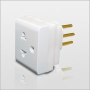
One central feature of any connector/plug is the pincount. The ubiquitous AC plugs we all know from an early age have 2 (or, more usually, 3) easily visible pins and of course the AC outlet is supposed to have the same number – and, intuitively, we know that the cable itself has the same number of wires. Depending on where you live, you may also be intimately familiar with adapters or conversion cables that have one type of plug on one end and a different type on the other. Here’s one AC adapter we’ve become used to here in Brazil, after the recent (and disastrous) change to the standard:

Even with such a simple adapter – if you open it, there’s just three metal strips connecting one side to the other – mistakes can be made. This specific brand’s design is faulty, assuming that the two AC pins are interchangeable. This is true for 220V, but in an area where 110V is used, neutral and hot pins will be reversed, which can be dangerous if you plug an older 3-pin appliance into such an adapter.

Still, my point here is that everybody is used to cables and adapters that are simple, inexpensive, and consist just of wires leading from one end to the other – after all, this is true for USB, Ethernet, FireWire, and so forth. Even things like DVI-VGA adapters seem to follow this pattern. But things have been getting more complicated lately. Even HDMI cables, which have no active components anywhere, transmit data at such speeds that careful shielding is necessary, and cable prices have stayed relatively high; if you get a cheap cable, you may find out that it doesn’t work well (or at all).

The recent Thunderbolt cables show the new trend. Thunderbolt has two full-duplex 10Gbps data paths and a low-speed control path. This means that you need two high-speed driver chips on each end of the cable (one next to the connector, one in the plug). This means that these cables sell in the $50 price range, and it will take a long time for prices to drop even slightly.

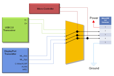
DisplayPort is an interesting case; it has 1-4 data paths that can run at 1.3 to 4.3Gbps, and a control path. The original connector had limited adoption and when Apple came out with their smaller mini version, it was quickly incorporated into the standard, and also reused for Thunderbolt. An even smaller version, called MyDP, is due soon. Analogix recently came out with an implementation of MyDP which they call SlimPort. MyDP is intended for mobile devices and squeezes one of the high-speed paths and the control paths down to 5 pins, allowing it to use a 5-pin micro-USB connector. Here’s a diagram of the architecture on the device side:

If you read the documentation carefully, right inside the micro-USB plug you need a special converter chip which converts those 3 signals to HDMI, and from then on, up to the other end of the cable, you have shielded HDMI wire pairs and a HDMI connector. Of course, this means that you can’t judge that cable by the 5 pins on one end, nor can you say that that specific implementation “transmits audio/video over USB”. It just repurposes the connector. Such a cable would, of course, be significantly more expensive to manufacture than the usual “wires all the way down” cable, and (because of the chip) even more than a standard HDMI cable.

Still referring to the diagram above, if you substitute the blue box (DisplayPort Transmitter) for another labeled “MHL Transmitter”, you have the MHL architecture, although some implementations use an 11-pin connector. Common to both MHL and MyDP is the need for an additional transmitter (driver) chip as well as a switcher chip that goes back and forth between that and the USB transceivers. This, of course, implies additional space on the device board for these chips, traces and passive components, as well as increased power consumption. You can, of course, put in a micro-HDMI connector and drive that directly, that would save neither space nor power.

Is there another way to transmit audio/video over a standard USB implementation? There are device classes for that, but they’re mostly capable of low-bandwidth applications like webcams; at least for USB2. Ah, but what of USB3? That has serious bandwidth (5Gbps) that certainly can accommodate large-screen, quality video, as well as general high-speed data transfer – not up to Thunderbolt speeds, though. You need a USB3 transceiver chip in the blue box above, and no switcher chip; USB3 already has a dedicated pin pair for legacy USB2 compatibility. All that’s needed is the necessary bandwidth on the device itself; and here’s where things start to get complicated again.

You see, there’s serious optimization already going on between the processor and display controller – in fact, all that is on a single chip, the SoC (System-on-a-Chip), labelled A6 in the iFixit teardown. Generating video signals in some standard mode and pulling it out of the SoC needs only a few added pins. If you go the extra trouble to also incorporate a USB3 driver on the SoC and a fast buffer RAM to handle burst transfers of data packets, the SoC can certainly implement the USB3 protocols. But – and that’s the problem – unlike video, that data doesn’t come at predictable times from predictable places. USB requires software to handle the various protocol layers, and between that and the necessity to, at some point, read or write that data to and from Flash memory, you run into speed limits which make it unlikely that full USB3 speeds can be handled by current implementations.

But, even so, let’s assume, for the sake of argument, that the A6 does implement all this and that both it and the Flash memory can manage USB3 speeds. Will, then, a Lightning-to-USB3 cable come out soon? Is that even possible? (You probably were wondering when I would get around to mentioning Lightning…)

Here’s where the old “wires-all-the-way-down” reflexes kick in, at least if you’re not a hardware engineer. To quote from that link:

Although it’s clear at this point that the iPhone 5 only sports USB 2.0 speeds, initial discussions of Lightning’s support of USB 3.0 have focused on its pin count—the USB “Super Speed” 3.0 spec requires nine pins to function, and Lightning connectors only have eight.

…The Lightning connector itself has two divots on either side for retention, but these extra electrical connections in the receptacle could possibly be used as a ground return, which would bring the number of Lightning pins to the same count as that of USB 3.0—nine total.

(…followed, in the comments, by discussions of shields and ground returns and…)

Of course, that contains the following failed assumptions (beyond what I just mentioned):

  1. Lightning is just a USB3 interface in disguise, and
  2. Cables and connectors are always wired straight-through, at most with a shield around the cable.
  3. If there are any chips in the connector, they must be sinister authentication chips!

These assumptions also underlie the oft-cited intention of “waiting for the $1 cables/adapters”. But, recall that Apple specifically said that Lightning is an all-digital, adaptive interface. USB3 is not adaptive, although it can be called digital in that it has two digital signal paths implemented as differential pairs. If you abandon assumptions 1 and 2, assumption 3 becomes just silly. Remember, the SlimPort designers put a few simple digital signals on the connector and converted them – just a cm or so away – into another standards’ differential wire pairs by putting a chip inside the plug.

So, summing up all I said here and in my previous posts:

  • Lightning is adaptive.
  • All 8 pins are used for signals, and all or most can be switched to be used for power. So it makes no sense to say “Lightning is USB2-only” or whatever. (But see update#5, below.)
  • The outer plug shell is used as ground reference and connected to the device shell.
  • At least one (probably at most two) of the pins is used for detecting what sort of plug is plugged in.
  • All plugs have to contain a controller/driver chip to implement the “adaptive” thing.
  • The device watches for a momentary short on all pins (by the leading edge of the plug) to detect plug insertion/removal. (This has apparently been disproved by some cheap third-party plugs that don’t have a metal leading edge.)
  • The pins on the plug are deactivated until after the plug is fully inserted, when a wake-up signal on one of the pins cues the chip inside the plug. This avoids any shorting hazard while the plug isn’t inside the connector.
  • The controller/driver chip tells the device what type it is, and for cases like the Lightning-to-USB cable whether a charger (that sends power) or a device (that needs power) is on the other end.
  • The device can then switch the other pins between the SoC’s data lines or the power circuitry, as needed in each case.
  • Once everything is properly set up, the controller/driver chip gets digital signals from the SoC and converts them – via serial/parallel, ADC/DAC, differential drivers or whatever – to whatever is needed by the interface on the other end of the adapter or cable. It could even re-encode these signals to some other format to use fewer wires, gain noise-immunity or whatever, and re-decode them on the other end; it’s all flexible. It could even convert to optical.

I’ll be seriously surprised if even one of those points is not verified when the specs come out. And this is what is meant by “future-proof”. Re-using USB and micro-USB (or any existing standard) could never do any of that.

Update: just saw this article which purports to show the pinouts of the current Lightning-to-USB2 cable. “…dynamically assigns pins to allow for reversible use” is of course obvious, if you put together the “adaptive” and “reversible” points from this picture of the iPhone 5 event. Regarding the pinout they published, it’s not radially symmetrical as I thought it would be (except for one two pins), so  I really would like a confirmation from some site like iFixit (I hear they’ll do a teardown soon). They also say:

Dynamic pin assignment performed by the iPhone 5 could also help explain the inclusion of authentication chips within Lighting cables. The chip is located between the V+ contact of the USB and the power pin of the Lightning plug.

I really see no justification for the “authentication chip” hypothesis, and even their diagram doesn’t show any single “power pin of the Lightning plug”. It’s clear that, once the cable’s type has been negotiated with the device, and the device has checked if there’s a charger, a peripheral or a computer on the other end, the power input from the USB side is switched to however many pins are required to carry the available current.

Update#2: I was alerted to this post, which states:

The iPhone 5 switches on by itself, even when the USB end [of the Lightning-to-USB cable] is not plugged in.

Hm. This would lend weight to my statement that a configuration protocol between device and Lightning plug runs just after plug-in – after all, such a protocol wouldn’t work with the device powered off. It also means that the protocol is implemented in software on the device side; otherwise they could just run it silently, until it really appears that the entire device needs to power up.

Still, there’s the question of what happens when the device battery is entirely discharged. I suppose there’s some sort of fallback circuit that allows the device to be powered up from the charger in that case.

Finally, I’ve just visited an Apple Store where I could get my first look at an iPhone 5. The plug is really very tiny but looks solid.

Update#3: yet another article reviving the authentication chip rumor. Recall how a similar flap about authentication chips in Apple’s headphone cables was finally put to rest? It’s the same thing; the chip in headphones simply implemented Apple’s signalling protocol to control iPods from the headphone cable controls. The chip in the Lightning connector simply implements Apple’s connector recognition protocol and switches charging/supply current.

Apple is building these chips in quantity for their own use and will probably make them available to qualified MFi program participants at cost – after all, it’s in their interest to make accessories widely available, not “restrain availability”.

Now, we hear that “only Apple-approved manufacturing facilities will be allowed to produce Lightning connector accessories”. That makes sense in that manufacturing tolerances on the new connector seem to be very tight and critical. Apple certainly wouldn’t want cheap knock-offs of the connector causing shorts, seating loosely or implementing the recognition protocol in a wrong way; this would reflect badly on the devices themselves, just as with apps. Think of this as the App Store for accessory manufacturers. 🙂

Update#4: new articles have come out with more information, confirming my reasoning.

The folks at Chipworks has done a more professional teardown, revealing that the connector contains, as expected, a couple of power-switching/regulating chips, as well as a previously unknown TI BQ2025 chip, which appears to contain a small amount of EPROM and implements some additional logic, power-switching, and TI’s SDQ serial signalling interface. SDQ also uses CRC checking on the message packets, so a CRC generator would be on the chip. Somewhat confusingly, Chipworks refer to CRC as a “security feature”, perhaps trying to tie into the authentication angle, but of course any serial protocol has some sort of CRC checking just to discard packets corrupted by noise.

Anandtech has additional information:

Apple calls Lightning an “adaptive” interface, and what this really means are different connectors with different chips inside for negotiating appropriate I/O from the host device. The way this works is that Apple sells MFi members Lightning connectors which they build into their device, and at present those come in 4 different signaling configurations with 2 physical models. There’s USB Host, USB Device, Serial, and charging only modes, and both a cable and dock variant with a metal support bracket, for a grand total of 8 different Lightning connector SKUs to choose from.

…Thus, the connector chip inside isn’t so much an “authenticator” but rather a negotiation aide to signal what is required from the host device.

Finally, there’s the iFixit iPod Nano 7th-gen teardown. What’s important here is that this is the thinnest device so far that uses Lightning, and it’s just 5.4mm (0.21″) thick. From the pictures you can see that devices can’t get much thinner without the connector thickness becoming the limiting factor.

Update#5: the Wikipedia article now shows a supposedly definite pin-out (and the iFixit iPhone 5 teardown links to that). Although I can’t find an independent source for the pin-out, it shows two identification pins, two differential data lanes, and a fixed power pin. Should this be confirmed it would mean that the connector is less adaptive in regarding to switching data and power pins; on the other hand, that pinout may well be just an indication of the default configuration for USB-type cables (that is, after the chips have negotiated the connection).

Boom: Teardown

1 comment

This is yet another follow-up to my posts about Apple’s new Lightning mobile connector.

The cool folks at iFixit have now published their comprehensive teardown of the iPhone 5. (Hopefully the other 2 new devices will also be done soon.)

Here’s a detail view of the Lightning connector inside the case: (click on all images to see the hires version from their site)

Notice two screws securing the connector body to the device case, and the metal bracket that keeps the other end from flexing. Here’s a closeup of the disassembled connector and of the plug:

Remember that the inside of the case is milled out of a solid block of metal, so this design looks to be much less breakable than the old 30pin version – I’ve been told that the tab end of the plug also feels very sturdy. Here’s a close-up of both connectors:

The space savings are considerable. I read that Apple has no plans to do a dock, so this looks to be a third-party opportunity. The previous connector had no serious protection against flexing, so previous docks had to grip the back and bottom of the device, which also led to a profusion of plastic dock adapters; Lightning docks should be able to get away with just a simple generic back support.

Confirming the rest of my speculations regarding the “adaptive” part of the Lightning interface will have to wait until the specifications leak… stay tuned.

Update: just saw a report about a teardown of the Lightning plug: “Peter from Double Helix Cables took apart the Lightning connector and found inside what appear to be authentication chips. He found a chip located between the V+ contact of the USB and the power pin on the new Lightning plug.”

It’s interesting how people assume that Lightning is just a pin-compatible extension of USB (which also explains why they feel that a cable should cost only a dollar or two). Note also that nobody knows for sure yet which pin is “the power pin”. Unfortunately the picture is very unclear ; it seems that there are three chips and a few passive components, at least on that side. Which, of course, goes far to confirm my hypothesis that the cable contains circuitry to tell the device which sort of adapter/cable is connected, as well as signal drivers/conditioners for USB2 (for this specific cable). The large chip, if it is really “directly in the signal path of the V+ wire”, probably switches the charging current to the appropriate pins on the device, once the interface has adapted to the cable – all this “authentication chip” paranoia is just – paranoia.

Update#2: it says here: “Included in the new high-tech part is a unique design which the analyst says is likely to feature a pin-out with four contacts dedicated to data, two for accessories, one for power and a ground. Two of the data transmission pins may be reserved for future input/output technology like USB 3.0 or perhaps even Thunderbolt, though this is merely speculation.”

See what I mean about people thinking that all pins are equal? What do they think that “adaptive” means, anyway?

Update#3: John Siracusa and Dan Benjamin agreed with my points in their latest talk show (references start just after the 49:00 mark) and they even sorta pronounced my name right. Thanks guys! 😉

Update#4: found a good discussion of the Lightning (published over a month ago!), with somewhat blurry pictures of a disassembled Lightning plug. They seem to match well with the linked pictures in the first update, above.

Update#5: my final summary. Please comment there, comments here are now closed.

Photos licensed by Creative Commons license. Unless otherwise noted, content © 2002-2024 by Rainer Brockerhoff. Iravan child theme by Rainer Brockerhoff, based on Arjuna-X, a WordPress Theme by SRS Solutions. jQuery UI based on Aristo.