This post has been updated several times (last update was on Feb.8, 2013); be sure to scroll to the end. Also see my final follow-up in 2014.
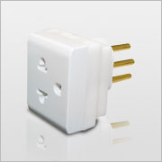
One central feature of any connector/plug is the pincount. The ubiquitous AC plugs we all know from an early age have 2 (or, more usually, 3) easily visible pins and of course the AC outlet is supposed to have the same number – and, intuitively, we know that the cable itself has the same number of wires. Depending on where you live, you may also be intimately familiar with adapters or conversion cables that have one type of plug on one end and a different type on the other. Here’s one AC adapter we’ve become used to here in Brazil, after the recent (and disastrous) change to the standard:

Even with such a simple adapter – if you open it, there’s just three metal strips connecting one side to the other – mistakes can be made. This specific brand’s design is faulty, assuming that the two AC pins are interchangeable. This is true for 220V, but in an area where 110V is used, neutral and hot pins will be reversed, which can be dangerous if you plug an older 3-pin appliance into such an adapter.
Still, my point here is that everybody is used to cables and adapters that are simple, inexpensive, and consist just of wires leading from one end to the other – after all, this is true for USB, Ethernet, FireWire, and so forth. Even things like DVI-VGA adapters seem to follow this pattern. But things have been getting more complicated lately. Even HDMI cables, which have no active components anywhere, transmit data at such speeds that careful shielding is necessary, and cable prices have stayed relatively high; if you get a cheap cable, you may find out that it doesn’t work well (or at all).
The recent Thunderbolt cables show the new trend. Thunderbolt has two full-duplex 10Gbps data paths and a low-speed control path. This means that you need two high-speed driver chips on each end of the cable (one next to the connector, one in the plug). This means that these cables sell in the $50 price range, and it will take a long time for prices to drop even slightly.
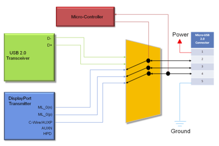
DisplayPort is an interesting case; it has 1-4 data paths that can run at 1.3 to 4.3Gbps, and a control path. The original connector had limited adoption and when Apple came out with their smaller mini version, it was quickly incorporated into the standard, and also reused for Thunderbolt. An even smaller version, called MyDP, is due soon. Analogix recently came out with an implementation of MyDP which they call SlimPort. MyDP is intended for mobile devices and squeezes one of the high-speed paths and the control paths down to 5 pins, allowing it to use a 5-pin micro-USB connector. Here’s a diagram of the architecture on the device side:

If you read the documentation carefully, right inside the micro-USB plug you need a special converter chip which converts those 3 signals to HDMI, and from then on, up to the other end of the cable, you have shielded HDMI wire pairs and a HDMI connector. Of course, this means that you can’t judge that cable by the 5 pins on one end, nor can you say that that specific implementation “transmits audio/video over USB”. It just repurposes the connector. Such a cable would, of course, be significantly more expensive to manufacture than the usual “wires all the way down” cable, and (because of the chip) even more than a standard HDMI cable.
Still referring to the diagram above, if you substitute the blue box (DisplayPort Transmitter) for another labeled “MHL Transmitter”, you have the MHL architecture, although some implementations use an 11-pin connector. Common to both MHL and MyDP is the need for an additional transmitter (driver) chip as well as a switcher chip that goes back and forth between that and the USB transceivers. This, of course, implies additional space on the device board for these chips, traces and passive components, as well as increased power consumption. You can, of course, put in a micro-HDMI connector and drive that directly, that would save neither space nor power.
Is there another way to transmit audio/video over a standard USB implementation? There are device classes for that, but they’re mostly capable of low-bandwidth applications like webcams; at least for USB2. Ah, but what of USB3? That has serious bandwidth (5Gbps) that certainly can accommodate large-screen, quality video, as well as general high-speed data transfer – not up to Thunderbolt speeds, though. You need a USB3 transceiver chip in the blue box above, and no switcher chip; USB3 already has a dedicated pin pair for legacy USB2 compatibility. All that’s needed is the necessary bandwidth on the device itself; and here’s where things start to get complicated again.
You see, there’s serious optimization already going on between the processor and display controller – in fact, all that is on a single chip, the SoC (System-on-a-Chip), labelled A6 in the iFixit teardown. Generating video signals in some standard mode and pulling it out of the SoC needs only a few added pins. If you go the extra trouble to also incorporate a USB3 driver on the SoC and a fast buffer RAM to handle burst transfers of data packets, the SoC can certainly implement the USB3 protocols. But – and that’s the problem – unlike video, that data doesn’t come at predictable times from predictable places. USB requires software to handle the various protocol layers, and between that and the necessity to, at some point, read or write that data to and from Flash memory, you run into speed limits which make it unlikely that full USB3 speeds can be handled by current implementations.
But, even so, let’s assume, for the sake of argument, that the A6 does implement all this and that both it and the Flash memory can manage USB3 speeds. Will, then, a Lightning-to-USB3 cable come out soon? Is that even possible? (You probably were wondering when I would get around to mentioning Lightning…)
Here’s where the old “wires-all-the-way-down” reflexes kick in, at least if you’re not a hardware engineer. To quote from that link:
Although it’s clear at this point that the iPhone 5 only sports USB 2.0 speeds, initial discussions of Lightning’s support of USB 3.0 have focused on its pin count—the USB “Super Speed” 3.0 spec requires nine pins to function, and Lightning connectors only have eight.
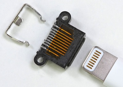
…The Lightning connector itself has two divots on either side for retention, but these extra electrical connections in the receptacle could possibly be used as a ground return, which would bring the number of Lightning pins to the same count as that of USB 3.0—nine total.
(…followed, in the comments, by discussions of shields and ground returns and…)
Of course, that contains the following failed assumptions (beyond what I just mentioned):
- Lightning is just a USB3 interface in disguise, and
- Cables and connectors are always wired straight-through, at most with a shield around the cable.
- If there are any chips in the connector, they must be sinister authentication chips!
These assumptions also underlie the oft-cited intention of “waiting for the $1 cables/adapters”. But, recall that Apple specifically said that Lightning is an all-digital, adaptive interface. USB3 is not adaptive, although it can be called digital in that it has two digital signal paths implemented as differential pairs. If you abandon assumptions 1 and 2, assumption 3 becomes just silly. Remember, the SlimPort designers put a few simple digital signals on the connector and converted them – just a cm or so away – into another standards’ differential wire pairs by putting a chip inside the plug.
So, summing up all I said here and in my previous posts:
- Lightning is adaptive.
- All 8 pins are used for signals, and all or most can be switched to be used for power. So it makes no sense to say “Lightning is USB2-only” or whatever. (But see update#5, below.)
- The outer plug shell is used as ground reference and connected to the device shell.
- At least one (probably at most two) of the pins is used for detecting what sort of plug is plugged in.
- All plugs have to contain a controller/driver chip to implement the “adaptive” thing.
- The device watches for a momentary short on all pins (by the leading edge of the plug) to detect plug insertion/removal. (This has apparently been disproved by some cheap third-party plugs that don’t have a metal leading edge.)
- The pins on the plug are deactivated until after the plug is fully inserted, when a wake-up signal on one of the pins cues the chip inside the plug. This avoids any shorting hazard while the plug isn’t inside the connector.
- The controller/driver chip tells the device what type it is, and for cases like the Lightning-to-USB cable whether a charger (that sends power) or a device (that needs power) is on the other end.
- The device can then switch the other pins between the SoC’s data lines or the power circuitry, as needed in each case.
- Once everything is properly set up, the controller/driver chip gets digital signals from the SoC and converts them – via serial/parallel, ADC/DAC, differential drivers or whatever – to whatever is needed by the interface on the other end of the adapter or cable. It could even re-encode these signals to some other format to use fewer wires, gain noise-immunity or whatever, and re-decode them on the other end; it’s all flexible. It could even convert to optical.
I’ll be seriously surprised if even one of those points is not verified when the specs come out. And this is what is meant by “future-proof”. Re-using USB and micro-USB (or any existing standard) could never do any of that.
Update: just saw this article which purports to show the pinouts of the current Lightning-to-USB2 cable. “…dynamically assigns pins to allow for reversible use” is of course obvious, if you put together the “adaptive” and “reversible” points from this picture of the iPhone 5 event. Regarding the pinout they published, it’s not radially symmetrical as I thought it would be (except for one two pins), so I really would like a confirmation from some site like iFixit (I hear they’ll do a teardown soon). They also say:
Dynamic pin assignment performed by the iPhone 5 could also help explain the inclusion of authentication chips within Lighting cables. The chip is located between the V+ contact of the USB and the power pin of the Lightning plug.
I really see no justification for the “authentication chip” hypothesis, and even their diagram doesn’t show any single “power pin of the Lightning plug”. It’s clear that, once the cable’s type has been negotiated with the device, and the device has checked if there’s a charger, a peripheral or a computer on the other end, the power input from the USB side is switched to however many pins are required to carry the available current.
Update#2: I was alerted to this post, which states:
The iPhone 5 switches on by itself, even when the USB end [of the Lightning-to-USB cable] is not plugged in.
Hm. This would lend weight to my statement that a configuration protocol between device and Lightning plug runs just after plug-in – after all, such a protocol wouldn’t work with the device powered off. It also means that the protocol is implemented in software on the device side; otherwise they could just run it silently, until it really appears that the entire device needs to power up.
Still, there’s the question of what happens when the device battery is entirely discharged. I suppose there’s some sort of fallback circuit that allows the device to be powered up from the charger in that case.
Finally, I’ve just visited an Apple Store where I could get my first look at an iPhone 5. The plug is really very tiny but looks solid.
Update#3: yet another article reviving the authentication chip rumor. Recall how a similar flap about authentication chips in Apple’s headphone cables was finally put to rest? It’s the same thing; the chip in headphones simply implemented Apple’s signalling protocol to control iPods from the headphone cable controls. The chip in the Lightning connector simply implements Apple’s connector recognition protocol and switches charging/supply current.
Apple is building these chips in quantity for their own use and will probably make them available to qualified MFi program participants at cost – after all, it’s in their interest to make accessories widely available, not “restrain availability”.
Now, we hear that “only Apple-approved manufacturing facilities will be allowed to produce Lightning connector accessories”. That makes sense in that manufacturing tolerances on the new connector seem to be very tight and critical. Apple certainly wouldn’t want cheap knock-offs of the connector causing shorts, seating loosely or implementing the recognition protocol in a wrong way; this would reflect badly on the devices themselves, just as with apps. Think of this as the App Store for accessory manufacturers. 🙂
Update#4: new articles have come out with more information, confirming my reasoning.
The folks at Chipworks has done a more professional teardown, revealing that the connector contains, as expected, a couple of power-switching/regulating chips, as well as a previously unknown TI BQ2025 chip, which appears to contain a small amount of EPROM and implements some additional logic, power-switching, and TI’s SDQ serial signalling interface. SDQ also uses CRC checking on the message packets, so a CRC generator would be on the chip. Somewhat confusingly, Chipworks refer to CRC as a “security feature”, perhaps trying to tie into the authentication angle, but of course any serial protocol has some sort of CRC checking just to discard packets corrupted by noise.
Anandtech has additional information:
Apple calls Lightning an “adaptive” interface, and what this really means are different connectors with different chips inside for negotiating appropriate I/O from the host device. The way this works is that Apple sells MFi members Lightning connectors which they build into their device, and at present those come in 4 different signaling configurations with 2 physical models. There’s USB Host, USB Device, Serial, and charging only modes, and both a cable and dock variant with a metal support bracket, for a grand total of 8 different Lightning connector SKUs to choose from.
…Thus, the connector chip inside isn’t so much an “authenticator” but rather a negotiation aide to signal what is required from the host device.
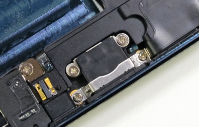
Finally, there’s the iFixit iPod Nano 7th-gen teardown. What’s important here is that this is the thinnest device so far that uses Lightning, and it’s just 5.4mm (0.21″) thick. From the pictures you can see that devices can’t get much thinner without the connector thickness becoming the limiting factor.
Update#5: the Wikipedia article now shows a supposedly definite pin-out (and the iFixit iPhone 5 teardown links to that). Although I can’t find an independent source for the pin-out, it shows two identification pins, two differential data lanes, and a fixed power pin. Should this be confirmed it would mean that the connector is less adaptive in regarding to switching data and power pins; on the other hand, that pinout may well be just an indication of the default configuration for USB-type cables (that is, after the chips have negotiated the connection).


