This is yet another follow-up to my posts about Apple’s new Lightning mobile connector.
The cool folks at iFixit have now published their comprehensive teardown of the iPhone 5. (Hopefully the other 2 new devices will also be done soon.)
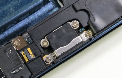
Here’s a detail view of the Lightning connector inside the case: (click on all images to see the hires version from their site)
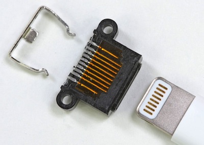
Notice two screws securing the connector body to the device case, and the metal bracket that keeps the other end from flexing. Here’s a closeup of the disassembled connector and of the plug:
Remember that the inside of the case is milled out of a solid block of metal, so this design looks to be much less breakable than the old 30pin version – I’ve been told that the tab end of the plug also feels very sturdy. Here’s a close-up of both connectors:
The space savings are considerable. I read that Apple has no plans to do a dock, so this looks to be a third-party opportunity. The previous connector had no serious protection against flexing, so previous docks had to grip the back and bottom of the device, which also led to a profusion of plastic dock adapters; Lightning docks should be able to get away with just a simple generic back support.
Confirming the rest of my speculations regarding the “adaptive” part of the Lightning interface will have to wait until the specifications leak… stay tuned.
Update: just saw a report about a teardown of the Lightning plug: “Peter from Double Helix Cables took apart the Lightning connector and found inside what appear to be authentication chips. He found a chip located between the V+ contact of the USB and the power pin on the new Lightning plug.”
It’s interesting how people assume that Lightning is just a pin-compatible extension of USB (which also explains why they feel that a cable should cost only a dollar or two). Note also that nobody knows for sure yet which pin is “the power pin”. Unfortunately the picture is very unclear ; it seems that there are three chips and a few passive components, at least on that side. Which, of course, goes far to confirm my hypothesis that the cable contains circuitry to tell the device which sort of adapter/cable is connected, as well as signal drivers/conditioners for USB2 (for this specific cable). The large chip, if it is really “directly in the signal path of the V+ wire”, probably switches the charging current to the appropriate pins on the device, once the interface has adapted to the cable – all this “authentication chip” paranoia is just – paranoia.
Update#2: it says here: “Included in the new high-tech part is a unique design which the analyst says is likely to feature a pin-out with four contacts dedicated to data, two for accessories, one for power and a ground. Two of the data transmission pins may be reserved for future input/output technology like USB 3.0 or perhaps even Thunderbolt, though this is merely speculation.”
See what I mean about people thinking that all pins are equal? What do they think that “adaptive” means, anyway?
Update#3: John Siracusa and Dan Benjamin agreed with my points in their latest talk show (references start just after the 49:00 mark) and they even sorta pronounced my name right. Thanks guys! 😉
Update#4: found a good discussion of the Lightning (published over a month ago!), with somewhat blurry pictures of a disassembled Lightning plug. They seem to match well with the linked pictures in the first update, above.
Update#5: my final summary. Please comment there, comments here are now closed.


